10+ i2c block diagram
To see the product features close this window. These devices feature R-tile transceivers with PCIe Gen5.
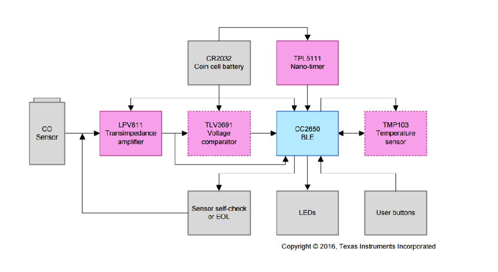
Always On Low Power Gas Sensing With 10 Year Coin Cell Battery Life Reference Design Electronics Lab Com
Display Your Work Easily With Our User-Friendly In-Editor Presentation Mode.
. External i2c connector block diagram josh lemaire 1 6. HMC Controller IP Core Block Diagram The HMC Controller IP core includes the following components. Block Diagram Sheet 3.
I2C Controller Block Diagram and System Integration Intel Agilex Hard Processor System Technical Reference Manual. BLOCK DIAGRAM FEATURES APPLICATIONS DESCRIPTION 10. Arm CoreSight Documentation 103.
High Level Block Diagram Figure 11. I2C stands for Inter-Integrated Circuit. As we know that the master initiates the data transfer the.
- 11 02_031712 a 4 3 2 1 sk2 9 8 7 6 5 4 3 2 10 1 sk1 sck sda ext_i2cvdd. FPGA Video Out IF Sheet 8. It is a bus interface connection protocol incorporated into devices for serial communication.
The below I2C protocol timing diagram gives a clear idea of the working of the protocol. I2C is a serial communication protocol so data is transferred bit by bit along a single wire the SDA line. I2C Protocol Programming in C for 8051 Interfacing of I2C protocol EEPROM with.
This architecture contains I2C slave and APB master. DDR3 Memory 34 Sheet 7. 15 The I2C master controller is comprised of three main blocks as described by Figure 1.
Users can configure the FPGA to. I2C Peripheral Block Diagram The I2C peripheral is compliant with the Philips Semiconductors. I2C Block Diagram X-Ref Target - Figure 22-2.
Projectname hw type. Ad Our Diagram Creator Makes It Easy To Share and Edit Your DiagramsWith Anyone Anytime. I2C Controller Block Diagram and System Integration Arria V Hard Processor System Technical Reference Manual.
Like SPI I2C is synchronous so the output of bits is synchronized to. Block Diagram The demonstration board showcases the features of the Intel Agilex I-Series device in the F2957 FBGA package. Figure 3 SPI-to-I2C Interface Top-Level Block Diagram Table 1 SPI Commands Command Message 0001 Write one or two bytes to I2C slave 0010 Read one or two bytes from I2C slave.
I2C_MASTER I2C Master Serial Interface Controller Rev. The circuit also has the extra functionality of operating as a level shifter if. FPGA Front End IF Sheet 4.
Two data paths an HMC TX path and an. Figure 2-3 is the block diagram of the board. UARTSPII2C MSP430F2254 16 MHz.
All the connections are established through the Arria 10 SoC FPGA device to provide maximum flexibility for users. Block Diagram Features Advanced High-speed Electrically-erasable Programmable Logic Device Superset of 22V10 Enhanced Logic Flexibility Backward Compatible with ATV750BBL. ECC Supported Memories 103.
Refer to Section 2 for detailed information about the architecture of the I2C peripheral. I2C Module Block Diagram Zynq UltraScale Device. P82B715 Block Diagram Block diagram.
The communication bridge between I2C and APB is shown in below figure. Display Your Work Easily With Our User-Friendly In-Editor Presentation Mode. It was originally designed by Philips.
I2c_slavevhd Top-level block i2c_slave_file_readervhd Reads the I2C bus signals from a text file i2c_slave_benchvhd Top-level test bench Functional Testing An example VHDL test bench is. In this article we will clarify how to build a bidirectional 2-bit mux circuit that can be used with I2C lines. 10 dac block diagram Rabu 21 September 2022 The block diagram of DAC is shown in the following figure.
FPGA DDR3 IF Sheet 5. These blocks are the master. Ad Our Diagram Creator Makes It Easy To Share and Edit Your DiagramsWith Anyone Anytime.
I2C Controller Block Diagram and System Integration Intel Arria 10 Hard Processor System Technical Reference Manual ID 683711 Date 8222022 Version Public Visible to Intel. The block diagram of I2C module is shown in This Figure. 10 i2c block diagram Sabtu 17 September 2022 The I 2 C reference design has a 7-bit address space with a rarely used 10-bit extension.
DDR3 Memory 12 Sheet 6.

Unique Wiring Diagram For Driving Lights Diagrams Digramssample Diagramimages Wiringdiagramsampl Relay Electrical Wiring Diagram Electrical Circuit Diagram

Ku19p Fpga System On Module Iwave Systems

Layerscape Ls1021a Smarc Som Iwave Systems

Dnwpuvlhyqxgsm

Matrix Vision Mvhyperion Technical Documentation Technical Data
Advanced And Scalable Som Hmi Solutions For Ev Charging Station Iwave Systems
What Is A Block Diagram In Signals And Systems And In Control Systems Quora

I Mx 8m Quad Quadlite Dual Smarc Som Iwave Systems
Arduino Fm Transmitter
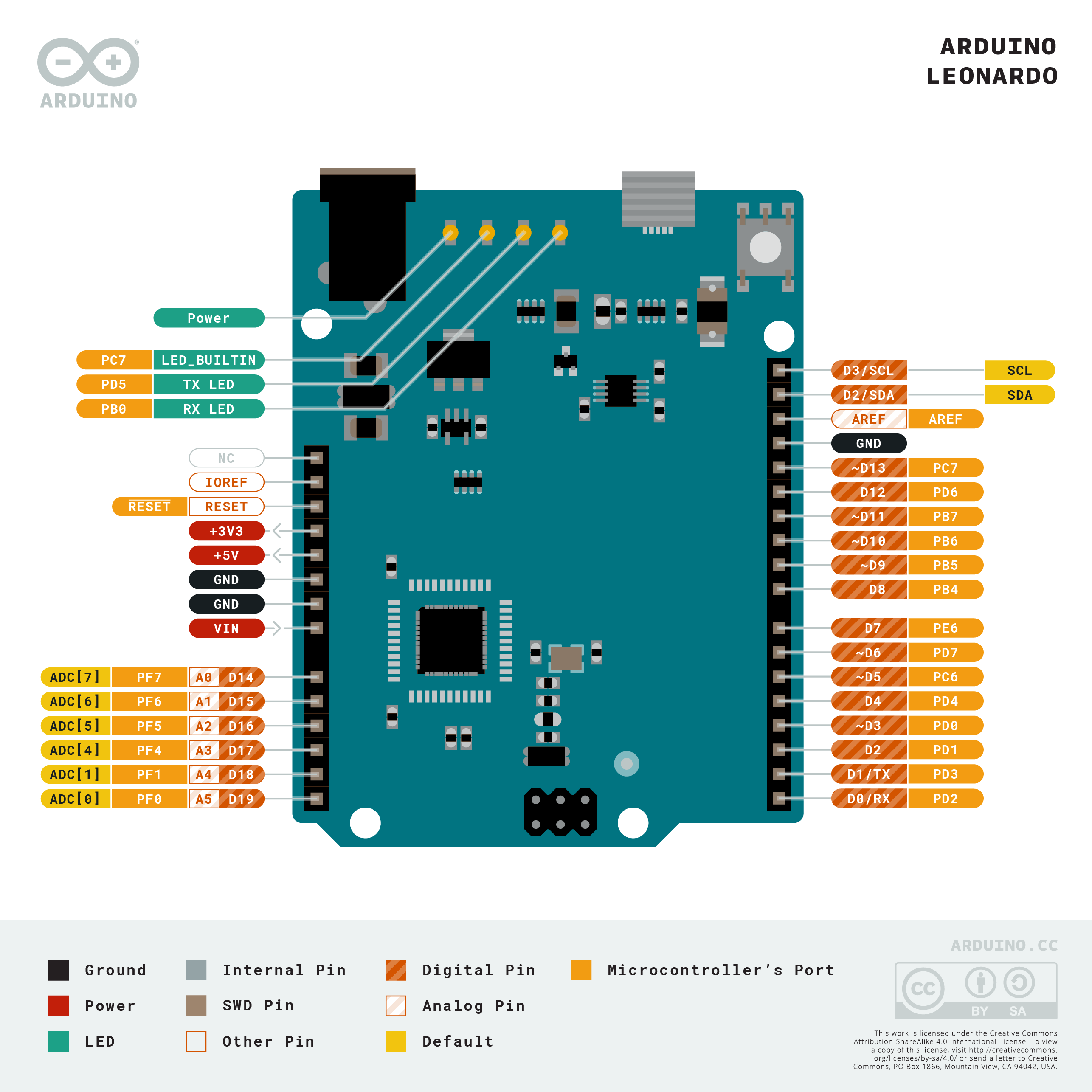
Arduino Leonardo With Headers Vilros Com
What Is A Block Diagram Of An Embedded System Quora

Matrix Vision Mvhyperion Technical Documentation Technical Data

Pin On Atmega328 Analogue I O Port Expander Using I2c Bus

I Mx 8 Qm Qp Pico Itx Sbc Iwave Systems
How To Draw A Block Diagram Of An Embedded System Quora

Pic Microcontroller Programming In C Example Pic Microcontroller Microcontrollers Electronic Circuit Projects

Image Result For Relay Wiring Diagram 5 Pin Electrical Circuit Diagram Circuit Diagram Electrical Diagram